#hardware prototyping
Explore tagged Tumblr posts
Visit Tumblr Blog
Explore Tumblr blogs with no restrictions, modern design and the best experience.
Last Seen Tumblr Blogs


Fun Fact
BuzzFeed published a report claiming that Tumblr was utilized as a distribution channel for Russian agents to influence American voting habits during the 2016 presidential election in Feb 2018.
Text
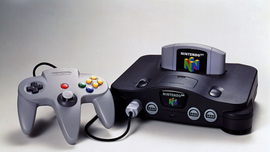
Nintendo 64
#nintendo 64#nintendo#nintendo aesthetic#hardware#tech#N64 controller#1995#1996#90s#90s aesthetic#prototype#N64
236 notes
·
View notes
Text
Solenoids go clicky-clacky 🔩🔊🤖
We're testing out an I2C-to-solenoid driver today. It uses an MCP23017 expander. We like this particular chip for this usage because it has push-pull outputs, making it ideal for driving our N-channel FETs and flyback diodes. The A port connects to the 8 drivers, while the B port remains available for other GPIO purposes. For this demo, whenever we 'touch' a pin on port B to ground, the corresponding solenoid triggers provide an easy way to check speed and power usage.
#solenoid#electronics#i2c#mcp23017#hardwarehacking#maker#embedded#engineering#robotics#automation#circuitdesign#pcb#microcontroller#tech#hardware#diyelectronics#electricalengineering#firmware#innovation#prototype#electromechanical#diy#electronicsproject#smarthardware#tinkering#gpio#fet#flybackdiode#programming#linux
44 notes
·
View notes
Text


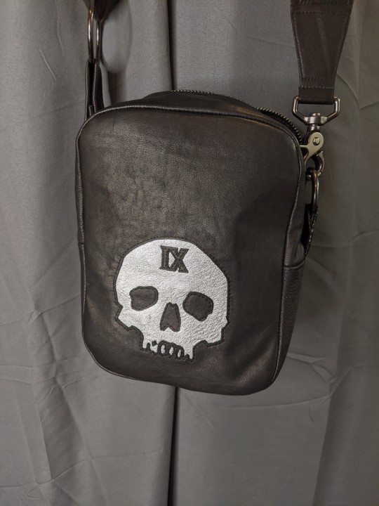
Pre-orders are open for the Jawless Skull ninth house leather crossbody bags! These will be hand made by me to hopefully ship in time for the holidays, so I'm only taking a limited number through 11/17.
There's some material customizability options AND some awesome griddlehark stickers you can also see in the store at mothgeist.com/shop ❤️✨
#the bag pictured is a prototype so theres going to be some material and hardware differences in the final product#including a fully removable shoulder strap!#bookblr#the locked tomb#gideon the ninth#harrow the ninth#nona the ninth#tlt#griddlehark#gideon nav#harrowhark nonagesimus
279 notes
·
View notes
Text

ID: A small screen and keyboard on top of a transparent clamshell case containing a battery and an Orange Pi Zero W 2 (a half credit card sized sbc). The device is running WezTerm (a modern terminal emulator) in qTile (a lightweight window manager) on Ubuntu
Running under its own power and enclosed in a smaller box we're getting close to where I want to be faster then expected.
39 notes
·
View notes
Text


124 notes
·
View notes
Text


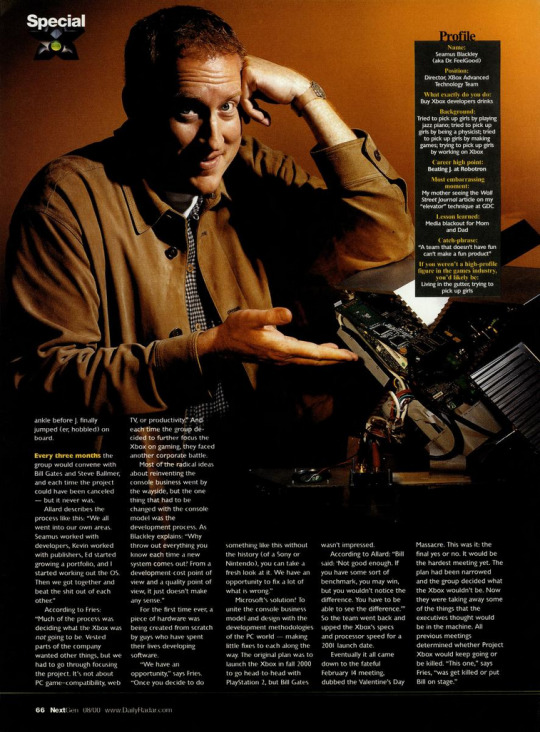
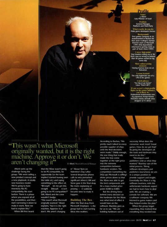

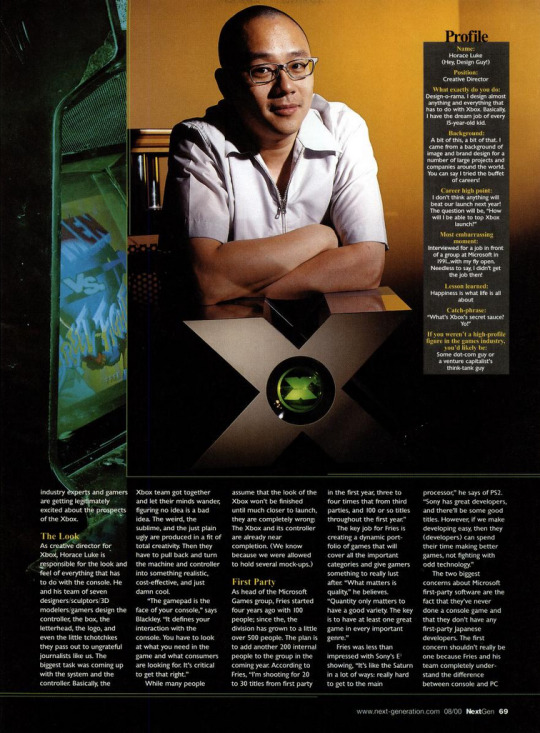


" Behind the scenes with the creators of the most powerful game machine on the planet! "
NextGen Magazine n68 - August, 2000.
#Microsoft#Microsoft Xbox#Xbox#OG Xbox#Xbox Prototype#DirectX Box#Big X#DirectX#Seamus Blackley#J Allard#Kevin Bachus#Horace Luke#Ed Fries#Channel Summers#Hardware
10 notes
·
View notes
Text
Mechanical Engineering Design Services
Expert hardware development & due diligence services at Glick Group Global ensuring strategic decisions. Explore our hardware development solutions for innovative and reliable products.
For more details, Visit: https://www.glickgroupglobal.com/
2 notes
·
View notes
Text
A call to help on repairing a one-of-a-kind prototype!
youtube
2 notes
·
View notes
Text

A close-up view of hands working on a microcircuit board, showcasing precision electronics engineering and prototyping. This image highlights the intricate process of assembling and testing electronic components, a key step in hardware design and development.
0 notes
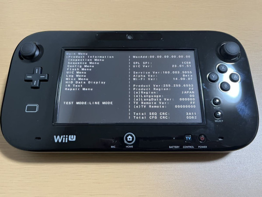
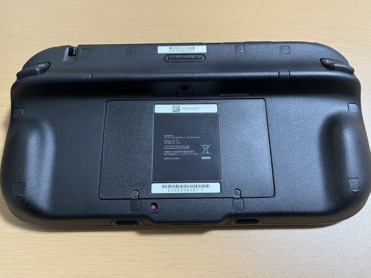
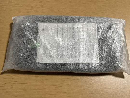
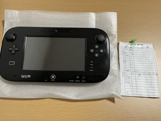
Text
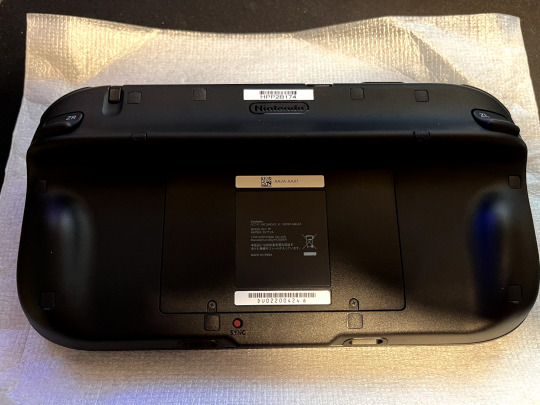
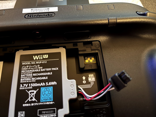
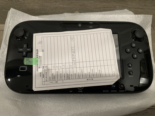
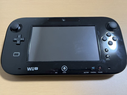
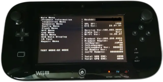
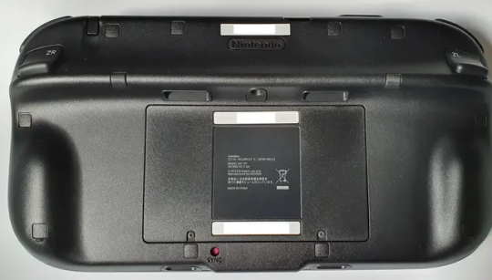
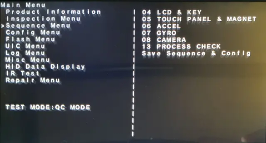
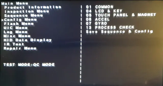
wii u gamepad factory test (proto?) firmware image dump
gamepad #1
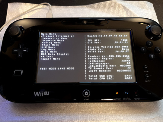


source: https://www.ebay.com/itm/405204224990
mirror: http://web.archive.org/web/20240920204350/https://www.ebay.com/itm/405204224990
info
listed by ebay user gaminggoodies_6
"Prototype (X11) WiiU Gamepad with factory test software"
gamepad #2
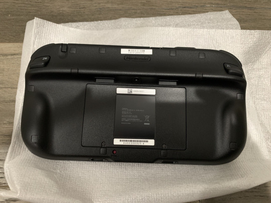
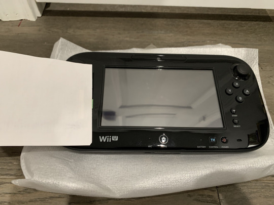

source: https://www.ebay.com/itm/166848537298
mirror: http://web.archive.org/web/20240920205744/https://www.ebay.com/itm/166848537298
info:
listed by ebay user whitecar12345
X11 gamepad
untested
gamepad #3

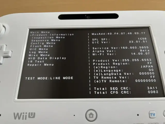
source: https://www.ebay.ca/itm/166566361641
mirror: http://web.archive.org/web/20240920215246/https://www.ebay.ca/itm/166566361641
most of the images are dead now, but using Highly Advanced Hackerman Techniques, i saw a few that i was able to archive... only two out of four images, images #1 and #3 respectively, but thankfully image #3 shows the relevant test menu. also, yes these are the highest resolution versions i could get, trust me i checked.
"Image 1 of 4" source: http://web.archive.org/web/20240920215055/https://i.ebayimg.com/images/g/QiAAAOSwWm9lsePB/s-l400.jpg
"Image 3 of 4" source: http://web.archive.org/web/20240920211535/https://i.ebayimg.com/images/g/QiEAAOSwWm9lsePC/s-l960.webp
info:
sold by ebay user re-toro_sushi_one-piece
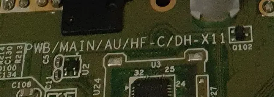
described as follows: "This is a factory test gamepad ..." "This is a prototype of the X11 that was actually used for performance evaluation at the Foxconn factory. A pre-finalize [sic] test menu is installed ..."
gamepad #4
source: https://www.ebay.com/itm/166777233237 mirror: http://web.archive.org/web/20240920223516/https://www.ebay.com/itm/166777233237
info:
sold by ebay user re-toro_sushi_one-piece
described as follows: "This is a factory test gamepad ..." "This is an X11 prototype that was actually used for performance evaluation in the Foxconn factory. The pre-finalize [sic] test menu is installed ..." "The packaging is from the factory, and the sheet used for the evaluation check is included. ..."
gamepad #5


source: https://x.com/PaulFelixKelly/status/1745260773897818353
info:
post by user PaulFelixKelly on Twitter / X
"Nintendo Wii U Tablet still in factory mode / Test Mode from the factory as these boards might have had defects and were binned before the normal software could be loaded onto them."
gamepad #6

source: https://www.reddit.com/r/wiiu/comments/14vsx0y/wii_u_gamepad_factory_mode/
posted by user FunkyGamer26
gamepad #7


source: https://consolevariations.com/collectibles/nintendo-wii-u-prototype-testpad alt source: https://consolevariations.com/profile/LinusDevTips/submissions
info:
images posted by user LinusDevTips
title: "Nintendo Wii U Prototype Testpad"; description: "Prototype testpad used for validation testing."
gamepad #8


source: https://www.neogaf.com/threads/wii-u-release-day-thread.499806/page-123#post-44484322
posted by user Tom_Cody
#wii u#wii u gamepad#prototype hardware#factory test firmware#wii u X11 gamepad proto (?)#odd retail hardware#in a few cases
1 note
·
View note
Text
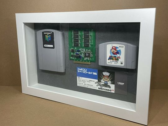
Nintendo 64 game cartridges and Super Mario 64 prototypes versions from 1995 or 1996.
#nintendo 64#nintendo#game cartridge#silicon board#tech#hardware#90s#retro gaming#collection#prototypes#nintendo aesthetic#N64
107 notes
·
View notes
Text
A4988 breakout prototype testing ⚙️🔧
We got our Allegro A4988 stepper driver breakout PCBs back and are ready to test them. First, we verified that STEP and DIR worked (yes!) and that the LEDs lit (yes, but we need to tweak the resistors to make the brightness even). Then we tried all of the stepper-settings, you can select 1, 4, 8, or 16-microsteps. All the sleep/reset/enable pins work. Finally, we checked the current limiting functionality with a potentiometer that can be twisted to select up to 2A current per coil. This directly affects the torque, so it's easy to test by verifying that we can stall the motor with hands or vise-grips. We'll order these with 2oz copper and get them into production next!
#a4988#stepperdriver#electronics#pcb#prototype#testing#breakoutboard#motorcontrol#microstepping#steppermotor#circuitdesign#electronicsengineering#makers#diyelectronics#hardware#engineering#currentlimiting#soldering#tinkering#pcblayout
44 notes
·
View notes
Text
The Rise of Arduino Compatible Boards - An Exploration of the Expanding Ecosystem
The Genesis of an Open Source Movement When Arduino was launched in 2005, it helped spawn the age of accessible, affordable microcontroller boards and platforms. By providing a common hardware and software standard that was simple to use but still powerful, Arduino opened the door for non-engineers and electronic hobbyists to easily create interactive projects and prototypes. This drastically lowered the barrier to entry for physical computing and embedded systems. Within a few years, the Arduino platform had grown into a thriving global community with developers of all skill levels sharing code, tutorials, and ideas. The Growing Demand Inspires New Options As Arduino gained popularity and demand increased, companies recognized an opportunity to expand the ecosystem. Rather than competing directly with Arduino, many started releasing boards that were compatible with the Arduino software and libraries. These clones and derivatives allowed users to benefit from Arduino's openness while also having alternative hardware options at lower price points or with additional features. Some boards were nearly identical clones while others incorporated unique enhancements. Regardless, their compatibility with the Arduino IDE gave users the flexibility to choose a board that best fit their specific needs and budgets. A Proliferation of Board Types and Form Factors Today, the variety of Arduino Compatible boards available is staggering. In addition to the classic Uno and Nano form factors, there are boards shaped as mini PCs, single-board computers, wearables, educational kits, drones, robots, and more. Each brings something new while still maintaining the foundational principles that make Arduino great. For example, some focus on size and portability while others emphasize power, connectivity, or cost. Educational boards make learning to code more interactive and hands-on. Industrial boards enable Arduino to be used in professional contexts that require certifications or rigorous testing. A World of Enhancements Beyond the Original Spec Many Arduino compatible boards one-up the original Arduino specs by including features like WiFi, Bluetooth, GPS, high-speed microprocessors, more memory and flash storage, additional input/output pins, and specialized sensors. Some push processing power to the level of Raspberry Pi while shrinking the board size. Others add compatibility for new languages beyond just C/C++. Interfaces like Ethernet, USB, and add-on shields expand what these boards can interface with. Many also supply dev kits with components, sensors, motors and displays to simplify prototyping of specific project types. Get more insights on Arduino Compatible
Unlock More Insights—Explore the Report in the Language You Prefer
French
German
Italian
Russian
Japanese
Chinese
Korean
Portuguese
Vaagisha brings over three years of expertise as a content editor in the market research domain. Originally a creative writer, she discovered her passion for editing, combining her flair for writing with a meticulous eye for detail. Her ability to craft and refine compelling content makes her an invaluable asset in delivering polished and engaging write-ups.
(LinkedIn: https://www.linkedin.com/in/vaagisha-singh-8080b91)

#Arduino Compatible#Microcontroller#Open-Source Hardware#Electronics#Prototyping#DIY#Hobbyist#Maker#Microcontroller Board#Arduino Uno
0 notes
Text
A4988 Pinout: A Comprehensive Guide
Discover the functionality and versatility of the Stepper Motor Driver Module A4988 Pinout, a crucial component in the world of robotics and automation. Let’s delve into the key details, with a specific focus on the A4988 pinout for a clearer understanding.
Stepper Motor Driver Module A4988
The A4988 is a stepper motor driver module that plays a pivotal role in controlling the precise movements of stepper motors. Whether you’re working on a 3D printer, CNC machine, or any other project requiring accurate motor control, the A4988 is a go-to choice.
A4988 Pinout Configuration
Understanding the A4988 pinout configuration is essential for effectively integrating the A4988 into your projects. Here’s a breakdown of the key pins:
MS1, MS2, MS3 (Microstep Resolution): These pins determine the microstep resolution, allowing you to set the stepping mode for the stepper motor. Configuring these pins enables fine-tuning of motor movement.
VMOT (Motor Power Supply Voltage): Connect this pin to the motor power supply voltage (typically 8V to 35V) to ensure the proper functioning of the stepper motor.
GND (Ground): Establish the ground connection by linking this pin to the ground of your power supply or microcontroller.
VDD (Logic Power Supply Voltage): Provide the logic power supply voltage (typically 3V to 5.5V) to this pin to power the internal logic circuitry of the A4988.
DIR (Direction Input): Control the direction of the stepper motor by connecting this pin to a digital output on your microcontroller.
STEP (Step Input): Trigger individual steps of the stepper motor by connecting this pin to another digital output on your microcontroller.
RESET (Reset Input): This pin resets the internal translator circuit, and it is optional to use.
SLEEP (Sleep Input): Putting the A4988 into sleep mode is achieved by connecting this pin to a digital high signal.
Read More: A4988 Pinout
#A4988#stepper-motor#microcontroller#Arduino#Raspberry-Pi#electronics#pinout#wiring#tutorial#DIY#project#hardware#software#programming#electronics-projects#microcontroller-projects#Arduino-projects#Raspberry-Pi-projects#open-source#maker#fabrication#prototyping#engineering#technology#innovation#learning#education
0 notes
Text

Explore elfminds extensive hardware development services, from idea validation to development. Our seasoned professionals specialize in digital and analog electronics, custom IoT sensors, and wireless network communication devices. Benefit from our collaborative approach, commitment to quality, and over 9 years of proven expertise.
0 notes
Text
Please signal boost: One-of-a-kind Broken Prototype S3 Chrome 460 Mega-infopost


(Yes, I know that is a very word salad-y post title.)
This is the S3 Chrome 460. It is currently nonworking. Nobody knows anything about it, and I’m trying to get in contact with any former S3 Graphics engineers that may be able to help.
What is known:
All “@” handles are in reference to users on Twitter.
As a whole, the Chrome 400 series utilized the Destination architecture, which was S3’s very first unified shader architecture capable of GPGPU tasks, much like Nvidia’s CUDA.
The Chrome 450/460 series utilized the mid-range “Destination 2” (D2) architecture, as opposed to “Destination 3” used by the low-end 430/440. As said by Loeschzwerg, there were no known high-end “Destination 1” architecture chip taped out. (https://twitter.com/Loeschzwerg_3DC/status/1683162950951903235)
The Chrome 450/460 was a 13x13mm (169mm2) die produced on the 90nm node by Fujitsu, and later TSMC. Strangely, the 430/440 series was produced on the much smaller 65nm node.
The Chrome 450/460 supported DX10, whereas the 430/440 supported DX10.1
The PCI device IDs for the Chrome 450/460 series are as follows:
o 9020, 9022, 9023, 9024, 9025 (http://listing.driveragent.com/c/pci/5333)
o The vendor ID for all chips is 5333 (S3 Graphics)
o There is one known beta driver that supports these device IDs (https://www.touslesdrivers.com/index.php?v_page=23&v_code=21175)
These PCI IDs appear to correspond to different die revisions
o Known existing die revisions present in collection: 86C920-921 (ID 9020), 86C922 (ID 9022 based on the cards owned by @Loeschzwerg_3DC), and 86C924 (can be assumed to be device ID 9024)
There are two “major” die revisions that exist.
o Revision 86C920-921 (I will refer to this as the “’920” revision) is most certainly the earliest revision, being physically larger in package size than all other revisions.
It also has a different pinout, and is produced by Fujitsu rather than TSMC, resulting in a greyish tint on the die rather than the blue tint of later revision chips.
The date code on all 86C920 chips (in my collection) reads “0727”, which implies that every ‘920 chip in existence was produced in a single batch on the 27th week of 2007, but cannot concretely prove so.
o Revision 86C922 (‘922) changes fabs from Fujitsu to TSMC, leaving the dies with a blueish tint and changing the pinout. This revision serves as the basis for all following revisions known to exist.
The date code on all 86C922 chips across my collection and Loeschzwerg’s appears to be 0738, implying that this revision was also produced in a single run much like its predecessor. (https://twitter.com/Loeschzwerg_3DC/status/1616750453500547072)
The 86C924 (‘924) revision is minor in comparison to the jump from ‘920 to ‘922, but interestingly the two in my collection have mismatching date codes—0728 and 0734. Unless I am reading the date codes wrong, this means that the ‘924 revision was produced either in two separate batches before the ‘922 run was done, or that perhaps it was continuously produced between the ‘920 and ‘922 revisions. I do not know what changes were made between ‘922 and ‘924.
o Almost all dies have a number and a letter, a word, or both written on them in permanent marker, likely for IDing which ones were being tested for what. The two words that appear the most often are “mem” (by far the most common) and “shift”. The letter “p” (pass?) also regularly appears.
There are three known Chrome 460 ES cards that exist: my broken early-revision ‘920 card, and Loeschzwerg’s two later-revision cards, one of which appears to be a 460 binned down to a 450.
There were rumors that the reason why the card was scrapped seemingly just before release was because its die became too expensive to produce (https://forum.beyond3d.com/threads/s3-excalibur-with-128-bit-mc-taped-out.42965/). There is zero confirmation or denial of this, and this rumor was said in passing on a thread discussing the follow-up Chrome 500 series (Excalibur architecture, which was later revealed to be a mildly tweaked at best Destination architecture).
The Chrome 460 (or at least, its ‘920 revision) gets hot very quickly, and may have been the reason for the switch to TSMC’s fabs.
o I believe that my card, despite having a heatsink and a fan blowing directly at it, likely died from overheating in the few minutes that it was running while I was collecting information and attempting to install an INF-modded 430/440 driver. It worked again after replacing the popped MOSFET and putting on the proper stock heatsink that it would’ve had mounted, but quickly died to a short a second time even with the new cooler. I still feel bad about this.
Most if not all Chrome 460 chips were acquired either directly through the S3/VIA/Centaur lab auction or through someone who attended the auction. The chips and card I own came from John at CPUShack, for example, and a number of others purchased miscellaneous 460s for their private collections from him.
o Loeschzwerg got his cards from a reseller who attended the 2021 Centaur auction just like I had.
And now, returning to my own broken card, to reiterate:
The card died to a short, and triggers the power supply’s OCP mode when the chip is installed on the board according to @dosdude1 . This does not happen when the chip is removed.
VCORE and GND were found by dosdude1 on the card’s footprint of the Chrome 460, and using that knowledge, the resistance from VCORE to GND on the chip itself was found:
o The original chip that was soldered to the card itself measured 1.5 ohms from VCORE to GND
o All other ‘920 chips between the ones in my collection and sent to dosdude1 as candidates for chip-swapping measure between 0.5 and 0.9 ohms, which I was told should be normal for graphics chips, but according to dosdude1 is still plenty low enough to trip the PSU’s OCP mode when installed.
Timeline
I originally purchased the card, alongside two “spare” ‘920 chips, two ‘922 chips, and two ‘924 chips, from CPUShack. The card had no heatsink included, so I had to make do with a chipset cooler (that honestly might have actually been better at cooling than the stock cooler) and a case fan.
o A few weeks after the purchase and arrival of the card, which by then had blown out its MOSFET and died short, I was able to buy a couple S3 Chrome 400-series coolers from CPUShack after he found them. Installing the cooler and replacing the MOSFET with an identical one salvaged off a Chrome 430 managed to get the card to work again for about half a minute from what I remember. However, I will also mention that the salvaged MOSFET came off a Chrome 430 that also died short. The MOSFET itself was undamaged, but the die itself appeared to be busted. I guess it was just an S3 thing during this generation.
o From what I remember, I filled out repair forms for both Louis Rossman and NorthRidgeFix, in hopes that a chip swap with one of the extra ‘920 dies I’d acquired at the time could bring the card back to life. In both cases I was turned down, though this was to be expected since there is zero documentation available for either the card or the chip itself.
o I was then able to get in contact with dosdude1, asking the same thing—just a chip swap was what I was hoping needed to be done. After some back and forth, I sent off the card, both of the extra ‘920 chips I had at the time, and some additional VRM MOSFETs that I’d bought after I’d run out of salvage chips.
o Shortly after the card and chips were mailed out, I came back to CPUShack asking if he had anymore Chrome 460 dies in stock. I proceeded to purchase all remaining chips he could find, which consisted of 10 ‘920 and 10 ‘922 revision dies.
o The chip swap would be completed with minimal issue, but the card unfortunately remained dead. It’s at this point where dosdude1 decided to probe for VCORE and GND, and in turn I measured out the resistance between the two on all ten of the ‘920 chips that had arrived by then, finding that they all read between 0.5 and 0.9 ohms. I do not know what the resistance from VCORE to GND is on the later die revisions, as the pinout was changed.
o Currently, dosdude1 is waiting for a buck regulator replacement to arrive after replacing the MOSFETs themselves yet again, finding in the process that the replacement MOSFETs I sent were faulty and… sending 12 volts straight into VCORE. That’s on me for buying them off Ebay. I did not know where else to look.
o Despite this, even after the faulty MOSFETs were replaced with tested working ones, the card continued to pull far too much current.
o Finally, as of now, he is still waiting for the buck regulator to arrive. There is no evidence that it is faulty as opposed to the MOSFETs, but neither of us have any clue what could be wrong anymore at this point aside from the dies themselves. It’s very much possible that one of the three dies in his possession have been fried to a crisp by that momentary 12v to VCORE in the split second before OCP kicked in, but even then after a non-faulty replacement was installed alongside a spare die it continues to trip the power supply’s OCP.
o I own 27 Chrome 460 dies across three revisions, 13 of which, counting the two sent to dosdude1 and the one installed on the card itself, are of the ‘920 revision that’s been causing myself and dosdude1 headaches for the better part of a year. Neither of us know what is wrong with the card, and outside of the discovery of the faulty “new” MOSFETs I’d sent, the only thing that appears to still be the issue are the dies themselves. They can’t all be bad, right?
Misc. info
My only lead on anyone that may be familiar with the S3 Chrome 460 is Bruce Chang of VIA Technologies. However, his email appears to only accept messages from others in the company.
Additional Photos


#not radioshack#techblog#youtube#my posts#S3 Chrome#S3 Chrome 460#prototype#prototype hardware#technology#prototype technology#graphics card#unreleased technology#tech blog#call for help#please signal boost
1 note
·
View note